Integration of the processor core with the NFC interface
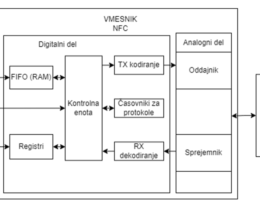
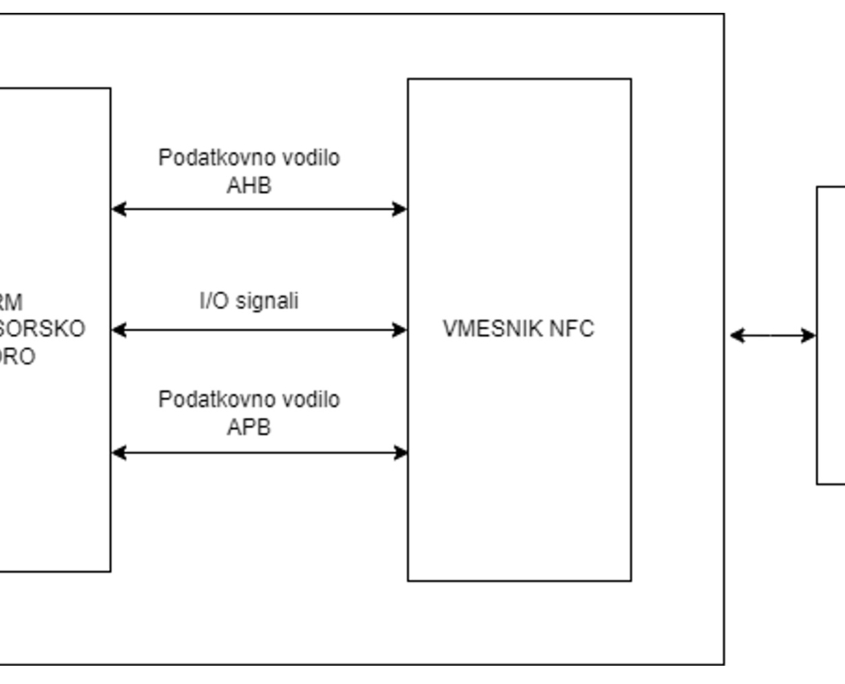
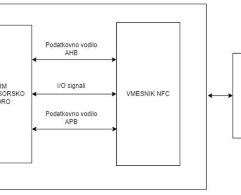
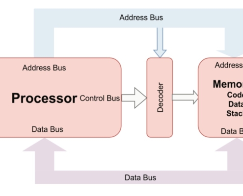
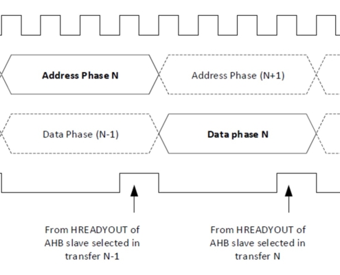
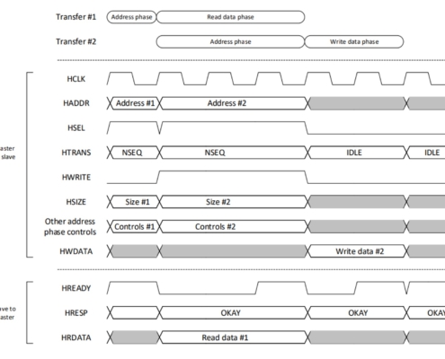
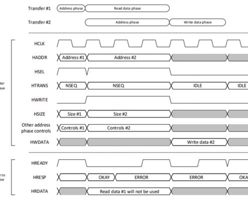
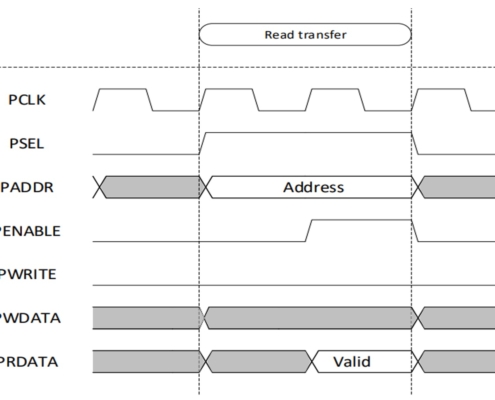
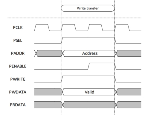
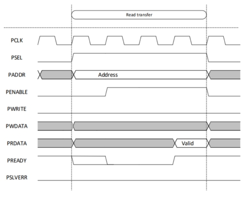
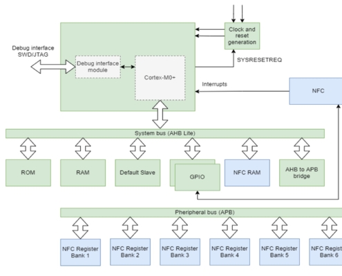
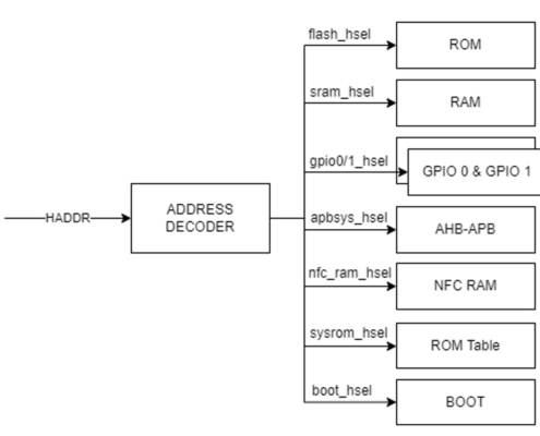
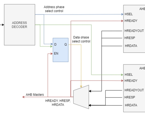
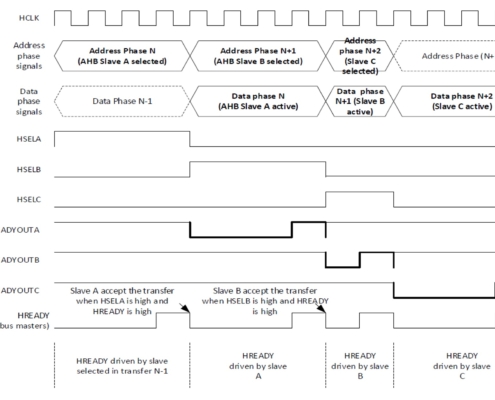
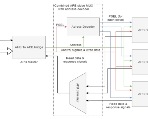
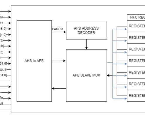
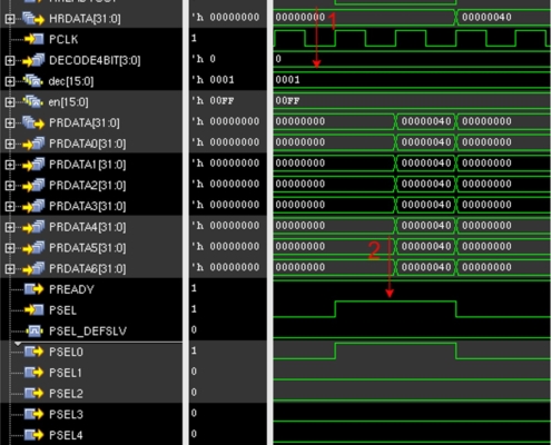
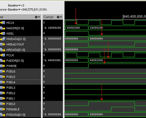
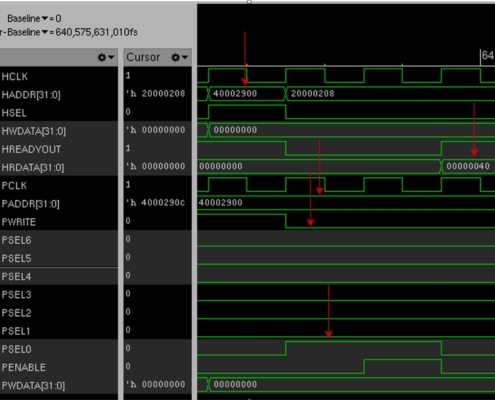
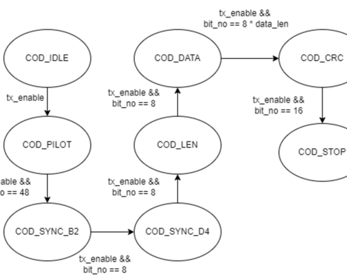
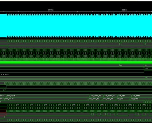
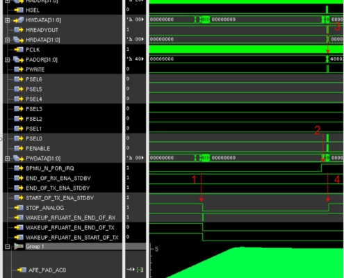
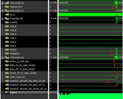
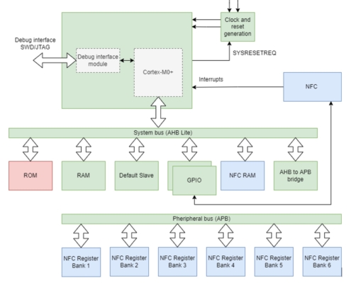
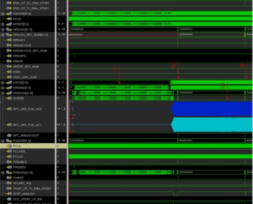
The NFC interface consists of a digital and analog part. In the analog part, there are blocks that take care of the correct reception and transmission of different types of modulations. This part contains various modulators, demodulators, power connectors and antenna connectors, through which the signal that we want to modulate or demodulate is transmitted or received. In the digital part, there is data control for encoding, decoding, registers through which we set the desired modulations, the states of the NFC interface, regardless of whether the NFC is powered by a battery or only via the field accepted by the NFC interface. The digital part also takes care of various functions, and various interrupts that take care of waking up the processor from sleep and various control blocks for the analog part. AHB and APB data buses are also located in the digital part. The AHB data bus takes care of communication with the internal memory of the NFC interface. The latter has its own memory, into which it writes data after reception, and in the case of transmission, it reads data from the memory, which it must transmit via the analog part, where it is then modulated according to the protocol. The APB data bus provides access to individual registers of the NFC interface, where protocols and interrupts are set. To connect the NFC interface to the processor core, we had to create a new AHB bus architecture, where we defined the individual locations of the system components. We connected the ROM to the buses, in which we store the program code in the initial stages of development, the RAM used for data storage, the default slave, two GPIO interfaces, the RAM NFC interface and the AHB-APB bridge. Signals for controlling the NFC interface were also connected to the GPIO interface.


